Customized PCB And PCB Manufacturer FR-4 PCB Circuit Board Design Manufacturing And Assembly
-
Highlight
Rigid Fr4 PCB Board
,Chrome Plating Fr4 PCB Board
,High Effective Circuit Board Assembly
-
Product NameCustomized PCB And PCB Manufacturer FR-4 PCB Circuit Board Design Manufacturing And Assembly
-
PCB MaterialFR-4, CEM-1, CEM-1 OR FR-4, FR4/ROGERS/PET/HDI/CEM/PI, Aluminium
-
Board Thickness0.2-6.0mm
-
PCB AssemblyCircuit Board-SMD-DIP-assembly
-
Place of OriginChina
-
Brand NameXHT
-
CertificationISO、IATF16949、RoSH
-
Model NumberXHT-FR-4 PCB Manufacturing-2
-
Minimum Order QuantityLow MOQ
-
PriceUS$ 1-5/Pcs
-
Packaging DetailsCarton with bubble bag
-
Delivery Time5-8 day
-
Payment TermsT/T, Western Union, MoneyGram
-
Supply Ability100000pcs/day
Customized PCB And PCB Manufacturer FR-4 PCB Circuit Board Design Manufacturing And Assembly

Customized PCB And PCB Manufacturer FR-4 PCB Circuit Board Design Manufacturing And Assembly
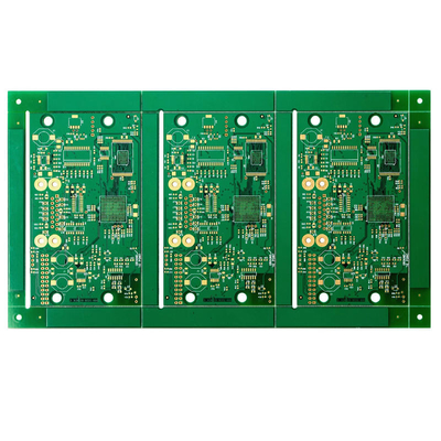
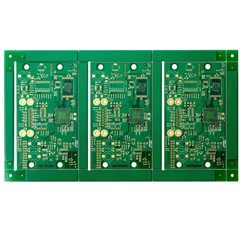
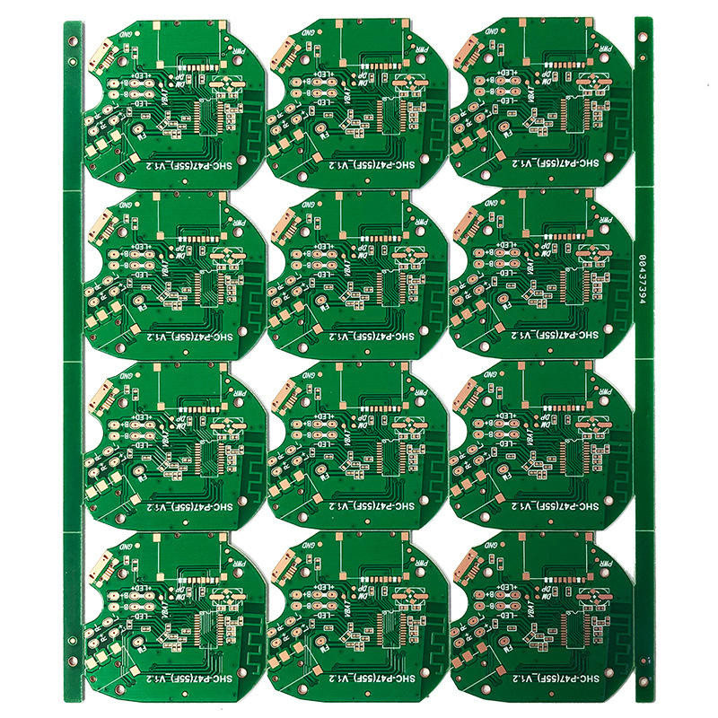
PCB board Manufacturing Customized PCB Rigid Printed Circuit Boards
In business since 2004, XHT mainly provides pcb fabrication and design service for customers from all over the world. We have ISO and UL certificate,and honored as HI-TECH enterprise by China goverment.
As a professional PCB factory , we can provide prototype and low-to-mid volume PCB board fabrication and design services for our customers. We are in Guangdong, China, which is the largest center of technology and electronics manufacturing in the world. Cooperating with our engineering team, quality team, these allow us to offer our customers low-cost, One-stop PCB Services.
we have strong supply chain for the electronic components.
- Provide full BOM component supply and part selection
- From the original factory and the first-level agents, the original authentic guarantee
- More than 50,000 kinds of components are always in stock
- Customers can buy on demand, no need to buy the whole package
PCB Capacities and Technical Specification
| NO. | Items | Capabilities |
| 1 | Layers | 2-68L |
| 2 | Maximum machining size | 600mm*1200mm |
| 3 | Board thickness | 0.2mm-6.5mm |
| 4 | Copper thickness | 0.5oz-28oz |
| 5 | Min trace/space | 2.0mil/2.0mil |
| 6 | Minimum finished aperture | 0. 10mm |
| 7 | Maximum thickness to diameter ratio | 15:1 |
| 8 | Via treatment | Via, blind&buried via, via in pad, Copper in via … |
| 9 | Surface finish/treatment | HASL/HASL lead free, Chemical tin, Chemical Gold, Immersion gold Inmersion Silver/Gold, Osp, Gold Plating |
| 10 | Base Material | FR408 FR408HR, PCL-370HR;IT180A, Megtron 6(Panasonic);Rogers4350, Rogers4003, RO3003, Rogers/Taconic/Arlon/Nelco laminate with FR-4 material(including partial Ro4350B hybrid laminating with FR-4) |
| 11 | Solder mask color | Green.Black.Red.Yellow.White.Blue.Purple.Matte Green. Matte Black |
| 12 | Testing Service | AOI, X-Ray, Flying-Probe, Function Test, First Article Tester |
| 13 | Profiling Punching | Routing,V-CUT,Beveling |
| 14 | Bow&twist | ≤0.5% |
| 15 | HDI type | 1+n+1,2+n+2,3+n+3 |
| 16 | Min mechanical aperture | 0.1mm |
| 17 | Min laser aperture | 0.075mm |
Advanced PCB Manufacturing and PCB Assembly Equipment
XHT has imported the advanced machinery from US,Japan,German and Israel to improve our production and technical ability.We have set a great example the PCB field of flying probe testing,buried and blind via and special controlled impedance.We have a highly developed R&D division which has helped our factory successfully produce mechanical micro via,high density impedance and HDI.
![]()
![]()
![]()
![]()
![]()
![]()
FAQ
| Q: How can we ensure our information should not let third party to see our design? XHT: We are willing to sign NDA effect by customer side local law and promising to keep customers data in high confidential level. |
| Q: What does XHT need for a customized PCB order? XHT : When you place a PCB order, the customers need to provide Gerber or pcb file. If you do not have the file in the correct format, you can send all the details related to the products. |
| Q: What is your inspection policy? How do you control the quality? XHT : In order to ensure the quality of PCB products, flying probe inspection is usually used; electrical fixtures, automatic optical inspection (AOI), BGA parts x-ray inspection, first article inspection ( FAI) etc. |
| Q: Can we inspect quality during production? XHT: Yes, we are open and transparent on each production process with nothing to hide. We welcome customer inspect our production process and check in house. |
Our products are sold all over the world, you can rest assured.